报告内容: 1. Prof. Mark Neisser: SPIE Microlithography Conference Review 2023年SPIE微光刻会议回顾 2. Dr. Elly Shi: Advanced lithography research and development for leading edge memory processes 应用于前沿存储器工艺的先进光刻工艺研发介绍 报告人简介: 1. Prof. Mark Neisser is the Director of the Photoresist lab at the Integrated Circuit Research Platform at the International Innovation Center of Tsinghua University, Shanghai. He has performed and managed R&D for most of his career, including at IBM, AZ Electronic Materials and SEMATECH. He is an expert in both lithography and lithographic materials such as photoresist, antireflective coatings, and spin on etch masks. He received his B.S. degree in chemistry from the Cornell University and his M.S. and Ph.D. degrees in chemistry from the University of Michigan. He is the author of more than 30 patents, over 100 journal papers and has co-authored two book chapters. He is the chairman of the IRDS roadmap lithography committee. He has been invited as Chair Professor in Tsinghua University since 2023。 2. 师江柳博士(Dr. Elly Shi) 2022年1月加入超弦存储器研究院。她曾经长期在美国应用材料公司和荷兰ASML公司工作,拥有20余年半导体设备、工艺研发及管理的跨国工作经验,特别专注于半导体光刻及相关技术领域。她毕业于天津大学,获得化学工程学士、硕士、博士学位。后赴荷兰代尔夫特理工大学(TU Delft) 微电子研究所 (DIMES)博士后工作,致力CMOS、Bipolar、SiGe工艺开发。 1999年加入阿斯麦(ASML),担任高级工程师至2007。此后她在应用材料(Applied Materials)中国和硅谷总部工作10年(2007-2017),作为高级技术专家负责工艺过程诊断、工艺控制、事业部,参与7nm CMOS先进工艺研发并负责图案成形(patterning)及相关量测和表征技术。她于2017回到阿斯麦(上海),先后担任客户技术支持部、电子束事业部中国市场战略营销部总监,负责为国内晶圆厂提供光刻、测量、控制、良率成套解决方案。 在阿斯麦和应用材料工作期间,她负责过国内外几十家半导体公司相关的工艺研发及量产技术支持,包括全球最先进的LOGIC,DRAM,NAND FLASH等工艺技术。 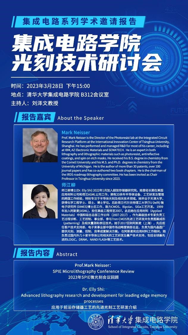
|












