简介: |
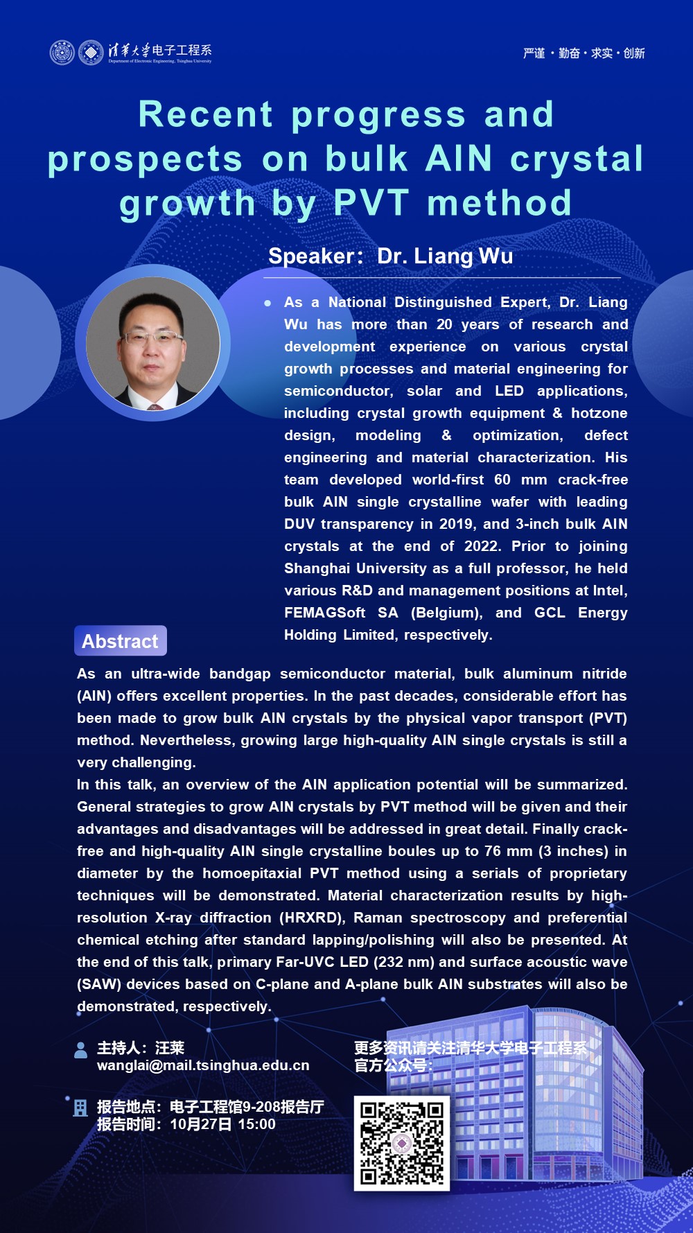
Abstract As an ultra-wide bandgap semiconductor material, bulk aluminum
nitride (AlN) offers excellent properties , such as wide bandgap(6.2eV), high thermal conductivity [340 w/(m·°C)], high breakdown field strength (15.4 MV/cm),
excellent UV transmittance, and chemical stability, and consequently
shows compelling advantages over other
competitors (SiC/GaN/Ga2O3) in power electronics as well as in deep-UV optoelectronics. The physical vapor transport (PVT) method is considered to be the most promising technique for bulk AlN growth. In the past decades, considerable effort has been made to grow bulk AlN crystals by the physical vapor transport (PVT) method. Nevertheless, growing large high-quality AlN single crystals is still a very challenging task from the viewpoint of both technological and scientific aspects. In this talk, an overview of the AlN application potential will be summarized. General strategies to grow AlN crystals by PVT method
will ?be given and their advantages and disadvantages will be
addressed in great detail. Finally crack-free and high-quality AlN
single crystalline boules up to 76 mm (3 inches) in diameter by the homoepitaxial PVT method using a serials of proprietary techniques will be demonstrated. Material characterization results by high-resolution X-ray diffraction (HRXRD), Raman spectroscopy and preferential chemical etching after standard lapping/polishing will also be presented. At the end of this talk, primary Far-UVC LED (232nm) and surface acoustic wave (SAW) devices based on C-plane and A-plane bulk AlN substrates will also be demonstrated, respectively.
Biography As a National Distinguished Expert, Dr. Liang Wu has more than 20 years of research and development experience on various crystal
growth processes and material engineering for semiconductor, solar
and LED applications, including crystal growth equipment & hotzone design, modeling & optimization, defect engineering
and material characterization. His team developed world-first 60 mm
crack-free bulk AlN single crystalline wafer with leading DUV
transparency in 2019, and 3-inch bulk AlN crystals at the end of 2022.
Prior to joining Shanghai University as a full professor, he held
various R&D and management positions at Intel, FEMAGSoft
SA(Belgium), and GCL Energy Holding Limited, respectively.
Dr. Liang Wu received his Ph.D., master and bachelor degree from Université catholique de Louvain, Tsinghua University and Dalian University of Technology,
respectively. He has been granted more than 60 patents and authored one book published in Germany. He contributed more than 100
journal / conference papers and invited/plenary keynote talks in leading national/international conferences.  学术海报20231027.jpg 学术海报20231027.jpg
|